
LearnElectronics India PCB Design & Embedded Internship 2026

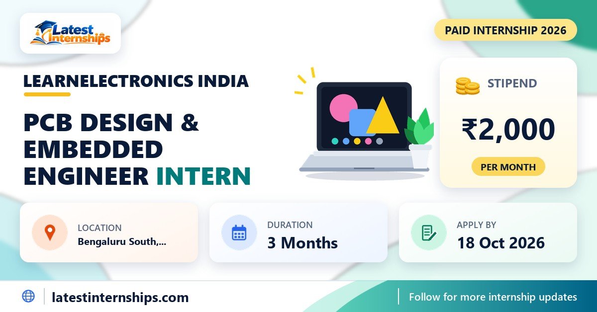
The LearnElectronics India PCB Design & Embedded internship is now open for applications on the AICTE Internship Portal. It pays ₹2,000 per month, runs for 3 months and is based in Bengaluru South, Karnataka. LearnElectronics India has 2 openings. Apply by 18 Oct 2026. It is at #11 in our list of the highest-paying internships we checked. LearnElectronics India posted it on 10 Oct 2026.
The listing asks for B.Tech / B.E / equivalent. It suits students who want hands-on work with C Programming, Python and Circuit Design. Below you will find the role, eligibility, stipend, important dates and the steps to apply, with the official link. Anything the listing does not mention is marked as not specified.
Internship Overview
Check these details before you apply.
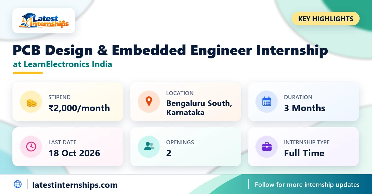
| Organization | LearnElectronics India |
|---|---|
| Internship Role | PCB Design & Embedded Engineer Intern |
| Stipend | ₹2,000 per month |
| Location | Bengaluru South, Karnataka |
| Work Mode | Not specified |
| Internship Type | Full Time |
| Duration | 3 Months |
| Openings | 2 |
| Last Date to Apply | 18 Oct 2026 |
| Apply On | AICTE Internship Portal |
About LearnElectronics India
The listing does not include a profile of LearnElectronics India. Look up the organization's own website and LinkedIn page to learn about its work before you apply.
Internship Details
Relocation, if needed, is arranged with the organisation.
Roles and Responsibilities
As per the listing, your work will include:
- Work on embedded system projects using microcontrollers (ESP32, Arduino, etc.)
- Design and develop PCBs using tools like EasyEDA, KiCAD, or similar
- Interface sensors, actuators, and communication modules (UART, I2C, SPI, etc.)
- Debug hardware and firmware issues
- Help with prototyping, testing, and documentation of projects
Read Next: Indian Army Mission Reliability Analytics for Artillery Internship
Domains and Departments
Engineering & Tech. Internship type Full Time.
C Programming,Python,Circuit Design,Arduino,ESP32,PCB Design. Desired attributes Communication Skills (Verbal & Writing), Coding Skills, Probleam Solving, Out of Box Thinking, Listening Skills, Analytical Ability, Team Work Skill, Time Management, Creative Skills, Learning Ability
Synopsis required
Eligibility Criteria
The listing sets these criteria:
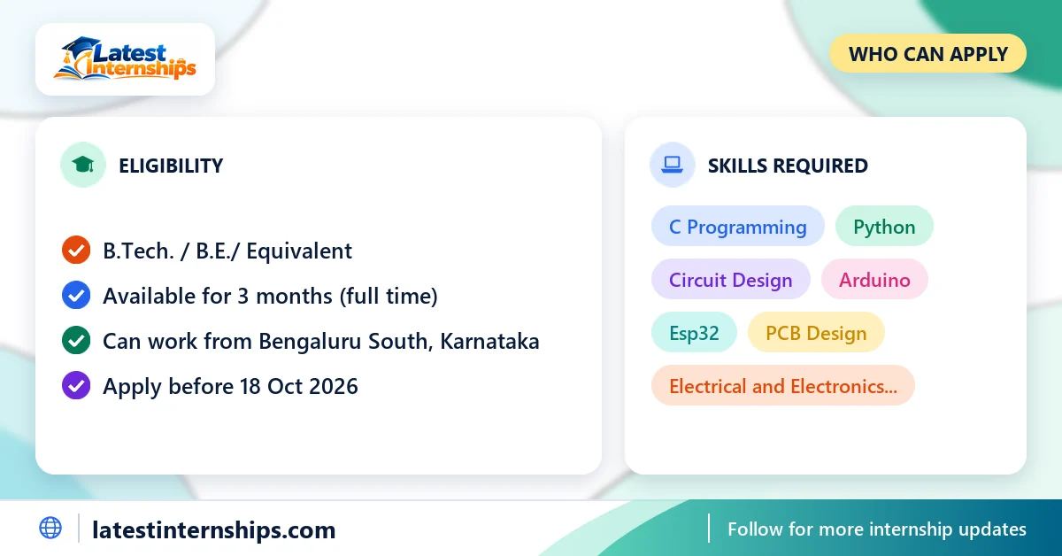
- Degree: B.Tech / B.E / equivalent
- and specialisation from Electrical and Electronics Engineering, Electronics and Communication Engineering, Electronics and Computer Engineering, Electronics and Telecommunication Engineering and Electronics Engineering
- You are from B.Tech. / B.E./ Equivalent
- You are available for duration of 3 Months
- You have relevant skills and interests
- Basic to intermediate knowledge of embedded systems
- Hands-on experience with PCB design tools (EasyEDA / KiCAD / others)
- Terms of engagement
- Internship Duration: 3–6 months, extendable based on performance and project requirements.
- Work Mode: On-site internship at the company's Bangalore office. Candidates must be based in Bangalore and willing to work from the office.
- Work Hours: Monday to Friday, 11:00 AM to 6:00 PM.
- Joining: Immediate joining preferred.
- As filed by learnelectronics india
Required Skills
Skills mentioned in the listing:
- C Programming
- Python
- Circuit Design
- Arduino
- Esp32
- PCB Design
- Electrical and Electronics Engineering
- Electronics and Communication Engineering
- Electronics and Computer Engineering
- Electronics and Telecommunication Engineering
Stipend and Benefits
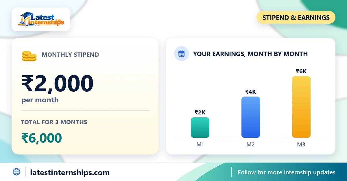
The listing gives a stipend of ₹2,000 per month.
| Per month | ₹2,000 |
|---|---|
| Total for 3 months | ₹6,000 |
Benefits
- 1. Monthly Stipend
- 2. Internship Completion Certificate
- 3. Practicle Learning Opportunity
Internship Duration and Mode
The internship runs for 3 months and is full time. It starts on 19 Oct 2026. The listing names Bengaluru South, Karnataka as the location. If you live elsewhere, check whether you can relocate for the full period.
On-site at Bengaluru South, Karnataka.
Important Dates
| Posted On | 10 Oct 2026 |
|---|---|
| Last Date to Apply | 18 Oct 2026 |
| Internship Start Date | 19 Oct 2026 |
Required Documents
No document list is given in the listing. An up-to-date resume (PDF) is the one file most forms ask for.
Selection Process
- Apply: Sign in with your student account and submit — about two minutes.
- Under review: LearnElectronics India screens every application directly on the portal.
- Shortlisted: You are notified on your dashboard and by e-mail.
- Interview: A short conversation or take-home task, online where possible.
- Selected: Offer letter and joining details arrive in your dashboard.
How to Apply for the PCB Design & Embedded Engineer Internship
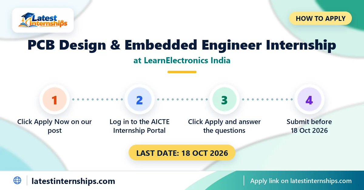
- Tap "Apply Now" below to open this internship on the AICTE Internship Portal.
- Log in with your student account. If you are new, register first with your college details.
- Read the details once more, then click Apply and answer the questions the company asks.
- Check your portal dashboard and email for updates on your application.
Important Official Links
- Official listing and application: PCB Design & Embedded Engineer internship listing on the AICTE Internship Portal
- AICTE Internship Portal: internship.aicte-india.org
- LearnElectronics India website: not given in the listing
The listing linked above has the complete description, which is shortened here.
Practical Tips for Applicants
- Complete your AICTE Internship Portal profile (college, course and year) before you apply, so the form goes through in one go.
- Keep a portfolio link ready (Behance, Dribbble or a PDF). Show 3-5 of your best designs.
- Keep your resume to one page and list the skills this listing asks for first.
- Do not wait for the last day. Some companies stop taking applications once they have enough.
- Before an interview, spend ten minutes reading about LearnElectronics India on its website and LinkedIn.
More Internships and Guides
Frequently Asked Questions
Short answers to what students usually ask about this role.
1How much does the LearnElectronics India PCB Design & Embedded internship pay?
The stipend is ₹2,000 a month. For the full 3 months, that is ₹6,000.
2Where is this internship located?
It is based in Bengaluru South, Karnataka.
3Who can apply for the PCB Design & Embedded Engineer internship?
It is open to students with B.Tech / B.E / equivalent. You also need to meet the availability conditions listed under the eligibility criteria.
4When does the application close?
Applications close on 18 Oct 2026. There are 2 seats in total.
5How can I apply?
Open the listing with the Apply Now button, sign in to the AICTE Internship Portal and submit your application there.
6Will I get a certificate?
A certificate is given after you finish the internship.
7Is there any fee to apply?
No fee is mentioned in the listing. If someone asks you to pay to confirm your selection, treat it as a warning sign.
Conclusion
This PCB Design & Embedded Engineer role at LearnElectronics India is a full time internship with a stipend of ₹2,000 per month, lasting 3 months. Check the official listing for any changes, then apply before the deadline.
About the Author
Disclaimer: This article is for information only. Latest Internships is an independent informational website and is not affiliated with AICTE or LearnElectronics India. Check the latest eligibility, stipend, deadlines and application details on the official website before you apply.



[…] LearnElectronics India PCB Design & Embedded Internship 2026 […]